
How can your businesses benefit from the Wafer Cassette Mapping?
- kensingtonlabsus

- Dec 29, 2020
- 2 min read
Talking about semiconductors production, silicon, the chemical element, is processed in the form of a wafer. The wafers are stored in the plastic cassettes during the production time under certain conditions and further processed in steps. As with the high demand for semiconductors, manufacturers think about automating the production process further.
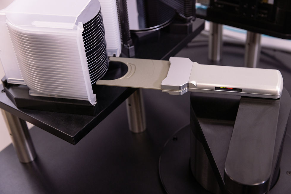
Now, you must know that the wafer front end movement between the semiconductor manufacturing can be procured with the wafer handling robots. The wafer handling automation is all based on the compliance arm for the robot assembly. The SCARA wafer handling robots gets processed in the horizontal work plane and the vertical work plane in 1DOF and 3DOF. So, these wafer handling robots can carry the throughputs of up to 350 wafers per hour with the positioning repeatability of 100 um.

Do you know that the wafer's optical alignment is gained by rotating the wafer, and the optical sensor's help to detect the wafer fiat's location? The wafers can be easily aligned concerning the tool of metrology. Do you know that the optical mean attains the active wafer alignment? You should know that the well known optical wafer alignment method includes the patterning alignment that checks out the wafer substrate. Such alignments can be seen within the microscope, which indulges a matching mark. Alignment can be further received when the two marks get in line with each other simultaneously. The submicron repeatability has been observed via the same method. The manual wafer registration via the optical alignment is a time-consuming process that is not practical for the in-line metrology applications. The automated optical alignment systems use robotic arms and vision systems to get the submicron wafer alignment. But you should know that it is pretty costly to implement in the metrology systems that don't consist of the imaging optics and the closed-loop controls for the wafer placement. If we actually work upon the advanced optical alignment system, it talks about the marks' interference patterns and can sub 20 nm wafer alignment. In fact, these systems are implemented in the multimillion-dollar nano-manufacturing tools. It requires good wafer alignment repeatability as the prices and resolution are larger than the general-purpose semiconductor metrology platform.

The wafer cassettes are mainly used for the purpose of storing and transport the wafers in the semiconductor manufacturing working process. The wafer cassettes are mostly known as the wafer carriers for many people. These are specially crafted to carry several wafers of equivalent sizes.
Let us discuss the dimensions of the wafer cassettes:
Pocket Spacing: It is calculated as the overall distance between each center line and every wafer pocket.
D1 Dimension: The dimension depicts the whole distance from one end of the cassette to the wafer pockets' centerline.
Pocket Flat: This is the term that supports each wafer pocket's width at the nano west distance.
The wafer cassette mapping and the wafer front end aids in turning most of it out of your business. Have the best and trustworthy assistance from Kensington Laboratories!
Don't delay to check out Kensington Laboratories that provides wafer handling automation to the industries at a modest rate.


Comments