Wafer Handling Equipment and Semiconductor Automation
- kensingtonlabsus

- May 31, 2020
- 2 min read
Updated: Dec 10, 2020
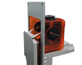
Wafer handling equipment has a tremendous burden of front-end module designs of equipment, due to which there is less tool productivity. There is no doubt that the span of manufacturing semiconductors goes to various stages, and it is a complex process. The company has to lay a huge emphasis on optimum quality and price in semiconductor equipment. In wafer mapping procedures of various kinds, 300mm FOUP proves effective.
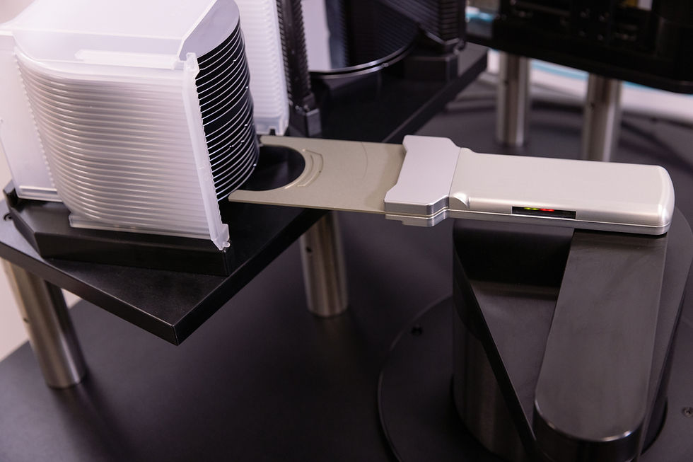
For businesses dealing with semiconductor front end, wafer handling robots are the best as they offer accuracy as well as repeatability. There is an increased workload in manual wafer handling, which can only be solved effectively by Wafer handling robots. A logical approach is provided by a wafer handling robots to decrease the manual workload.
Current wafer handling robots can pick and place 300mm wafers in a sequence in a repeated manner. Wafers are picked and placed based on the location of the joint. A typical sequence involves

Extend to wafer pick location
Pick wafer
Retract to a safe position
Extend arm to place location
Place wafer
Repeat
Wafer handling robots perform tasks in a series to make sure the robot follows the instructions, and it has reached the point where it has been directed to go. When the time to do such tasks decreases, the output is increased, and that's what the industry is working on- to increase the output by decreasing the time taken.
Some Features of Wafer Handling Robots
The central benefit of wafer handling robots is that they complete the task in an efficient manner, which otherwise consumes plenty of time manually. Wafer handling robots are extremely accurate and have the ability to complete the task in less time. The collisions of wafer handling robots are avoided by monitoring the electrical overhead and by safety scanning.
Throughout the years, there have been significant advancements in wafer handling robots. Now, we see there are high throughput and superior performance, and these features are the highlights, which make wafer handling robots a favorite of manufacturing firms.
The commands of wafer handling robots are very easy to learn; with some research, they can be self-learned. These robots can easily identify fault and recovery; that's why they are a preferred choice of the industries.
Wafer mapping sensors are stress-free to maintain, and they are easy and safe to use. Wafer mapping sensors reduce the manufacturing cost tremendously as they improve efficiency. The assimilated barcode reader or the off-axis reader, along with the direct optical algorithm of the entire involved axis, tends to the recurrence of wafer placement. This trait makes wafer mapping one of the best in the competition. To analyze data, wafer handling software is widely used.

The Fabrication of a Semiconductor Device
The manufacturing phase of an integrated circuit is divided into two phases. The first phase is wafer fabrication; it is incredibly sophisticated and also a very complicated process of manufacturing the silicon chip. Assembly is the second phase, and it is the extremely accurate and automated process of packaging the die. Those two phrases are termed as semiconductor front end and "Back-End." They incorporate two test steps: wafer probing and final test.


Comments