

Why Precision Motion Control Is Essential for Semiconductor Equipment

The global rush to secure sub-2nm node architectures has fundamentally changed the parameters of modern chip manufacturing. As fab facilities integrate Extreme Ultraviolet (EUV) lithography and high-numerical-aperture systems, the margins for physical deviation have shrunk from the nanoscale down to angstrom-level thresholds.
Within this environment, the mechanics of shifting silicon can no longer rely on traditional motorized tracks. Reaching these extreme production tolerances requires a total reliance on high-performance mechanical integration, which is exactly why precision motion control has transitioned from a standard machinery specification into the absolute baseline of modern fab viability.

Navigating the Sub-Nanometer Frontier
The primary driver behind this shift is the relentless reduction of feature sizes on modern transistors. Fabricating these dense architectures requires exposing, etching, and measuring microscopic patterns across a multi-layered silicon wafer with zero structural drift.
During critical front-end processes, an internal XY precision stage must guide the silicon underneath optical lenses with flawless repeatability. Any micro-vibration, thermal expansion, or minor tracking error during this journey immediately causes pattern overlay faults, ruining the entire wafer
Achieving sub-nanometer positioning accuracy is no longer just about moving a component from point A to point B - it requires dynamically neutralizing structural resonance and atmospheric disturbances in real time. Because a single modern fab line represents billions of dollars in capital investment, preventing mechanical deviation is the single most effective way to secure high operational yields and avoid catastrophic material waste.
Throughput Optimization in Advanced Packaging

The technical challenge expands exponentially as advanced chip design shifts toward heterogeneous integration - stacking multiple specialized dies into a single package. This architecture relies heavily on sophisticated high-speed wafer processing routines where throughput and precision must scale simultaneously.
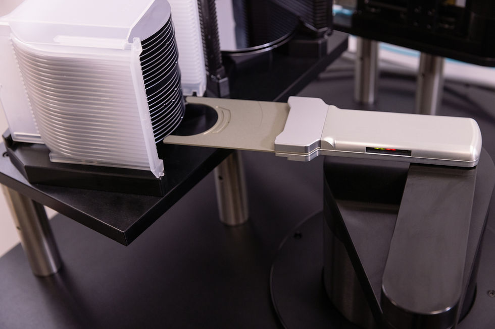
Modern assembly lines cannot afford to sacrifice speed to ensure accuracy. Advanced systems must accelerate at multiple Gs, stop instantly without structural ringing, and execute automated scans without dropping throughput.Without advanced precision motion control systems handling these intense mechanical profiles, the rapid pick-and-place movements required for advanced packaging would cause severe mechanical wear and drastically reduce equipment lifespans.
Sustaining Yields via Intelligent Automation
Integrating software-driven intelligence directly into the manufacturing footprint is a major step forward for modern semiconductor automation. Modern fabrication tools use closed-loop control systems running on fast industrial networks like EtherCAT to read high-resolution optical encoder feedback and adjust motor parameters on the fly. This real-time adaptation protects the physical wafer from micro-frictional friction changes and structural aging. Total global investments in fabrication infrastructure are projected to hit $139 billion in 2026, making long-term mechanical reliability a core financial necessity. By utilizing advanced physical models and adaptive filtering, motion networks predict mechanical friction and wear before they impact production quality. This predictive approach keeps lines running smoothly and prevents unexpected downtime.
Mitigating Thermal and Environmental Disturbances
Environmental stability inside the fab is just as vital as raw mechanical rigidity. At angstrom thresholds, minor atmospheric variations can rapidly degrade positioning accuracy and corrupt complex exposures.
Active Thermal Dissipation- Modern architectures integrate cooling channels directly into motor frames to eliminate core thermal expansion before it warps the stage.
Vacuum and Particle Control- Operating within cleanrooms requires highly specialized precision motion control designs that completely prevent outgassing and eliminate micro-frictional particulate debris.
Parasitic Magnetic Isolation- Actively shielding stage components ensures stray electromagnetic interference never disrupts sensitive electron-beam inspection processes.
Concluding Thoughts
As the industry pushes the absolute physical limits of silicon fabrication, structural stability remains a critical gatekeeper for scaling performance. Equipment manufacturers cannot afford any weakness in their positioning subsystems. Achieving these extreme metrics requires a deep, uncompromising focus on structural design, which is why top-tier tool builders continuously collaborate with established engineering partners. For organizations looking to deploy next-generation wafer lines, Kensington Laboratories remains a trusted leader in precision robotics and automation solutions for the semiconductor industry, delivering the sub-nanometer reliability required to power the future of global computing.


Comments